
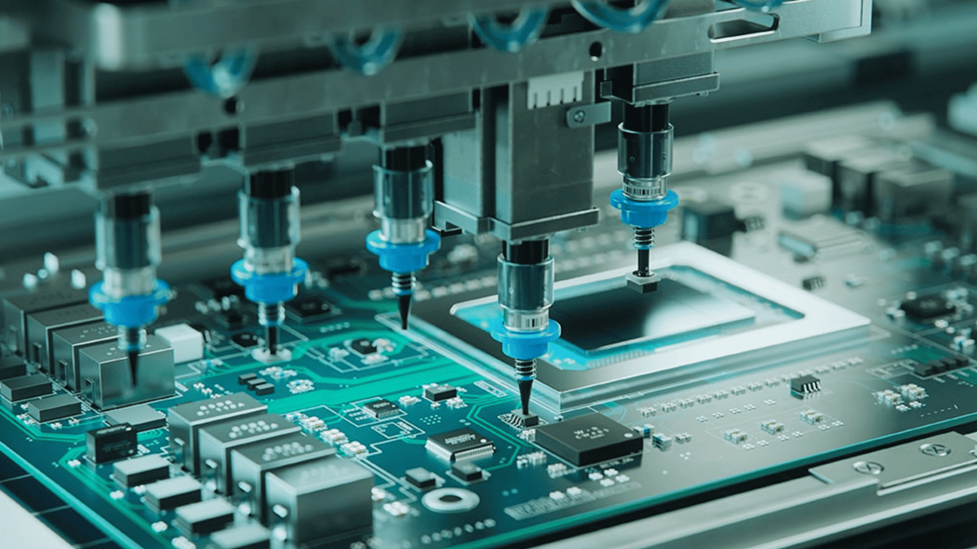





Every time you unlock your phone, stream a video, drive an electric vehicle, or use an AI-powered tool, you rely on billions of tiny semiconductor components working behind the scenes.
Semiconductors power the technology people use every day, from smartphones and laptops to electric vehicles and AI systems.
These tiny components enable devices to process, store, and transfer information efficiently.
The semiconductor manufacturing process turns silicon wafers into finished chips through fabrication, testing, and packaging.
With continuous innovations in manufacturing technology, companies can create smaller, faster, and more energy-efficient chips that support the growth of modern electronics and emerging technologies
Quick Answer: What Is Semiconductor Processing?
Semiconductor processing is the series of manufacturing steps used to create integrated circuits (ICs) on silicon wafers.
It involves adding, removing, and modifying extremely thin layers of materials to build microscopic structures that allow chips to perform electronic functions.
Manufacturers use several advanced techniques to create these circuits, including lithography, which transfers circuit patterns onto wafers, and etching, which removes unwanted materials.
These processes convert raw silicon wafers into functional semiconductor chips used in modern electronic devices.
How Are Semiconductors Made?
Semiconductors are made through a highly controlled manufacturing process that turns raw silicon into finished chip components used in electronic devices.
The journey begins with creating and preparing silicon wafers, which are then processed through multiple fabrication steps to build microscopic circuits.
After the circuits are formed, each chip undergoes testing to identify defects and verify performance.
The final stages involve semiconductor packaging, where chips are protected and connected for practical use, followed by final inspection to ensure quality, reliability, and readiness for integration into devices.
The main phases include wafer fabrication, testing, packaging, and final inspection.
What Are the 4 Stages of Semiconductor Manufacturing?
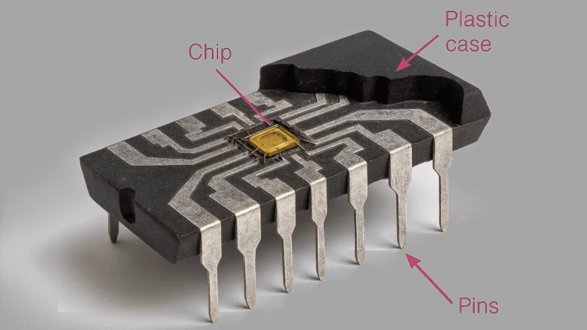
Semiconductor manufacturing involves several carefully controlled stages that turn chip designs into reliable electronic components.
- Design and Mask Creation: Engineers create chip layouts, simulate designs, and prepare photomasks used during fabrication.
- Wafer Fabrication: Silicon wafers are processed using deposition, lithography, etching, and doping to build circuits.
- Assembly and Packaging: Individual chip dies are placed into protective packages to improve durability and performance.
- Testing and Quality Control: Finished chips are tested for defects, performance, and reliability before shipment.
What Is Semiconductor Packaging?
Semiconductor packaging is the process of placing individual chip dies into protective cases that provide support, electrical connections, and protection from damage.
It is a critical manufacturing stage because it allows chips to function properly inside electronic devices.
Packaging helps manage heat and improves electrical performance by enabling efficient signal transfer between chip components.
It also increases device reliability by protecting delicate semiconductor parts from moisture, heat, and physical stress.
Semiconductor Manufacturing vs. Semiconductor Packaging
Semiconductor manufacturing and packaging are connected but serve different purposes, with each stage helping create reliable, high-performance chips for modern devices.
| Aspect | Semiconductor Manufacturing | Semiconductor Packaging |
|---|---|---|
| Purpose | Creates microscopic circuits on silicon wafers. | Protects chips and enables external connections. |
| Main Process | Uses lithography, deposition, etching, and doping to build chip structures. | Places chip dies into protective packages with electrical connections. |
| Output | Produces semiconductor dies with functional circuits. | Produces finished chips ready for use in devices. |
| Focus | Improves chip performance, size, and efficiency. | Enhances durability, heat management, and reliability. |
What Is a Semiconductor Fab or Fabrication Plant?
A semiconductor fab, or fabrication plant, is a specialized facility where silicon wafers are transformed into finished semiconductor chips through highly precise manufacturing processes.
These facilities use advanced equipment for steps such as lithography, deposition, etching, and testing.
Fabs require extremely clean environments called cleanrooms to prevent tiny particles from affecting chip production.
Building and operating a semiconductor fab requires significant investment, advanced technology, and skilled engineers.
These facilities are essential for producing the chips used in smartphones, computers, electric vehicles, AI systems, and other modern technologies.
Understanding the Semiconductor Manufacturing Process
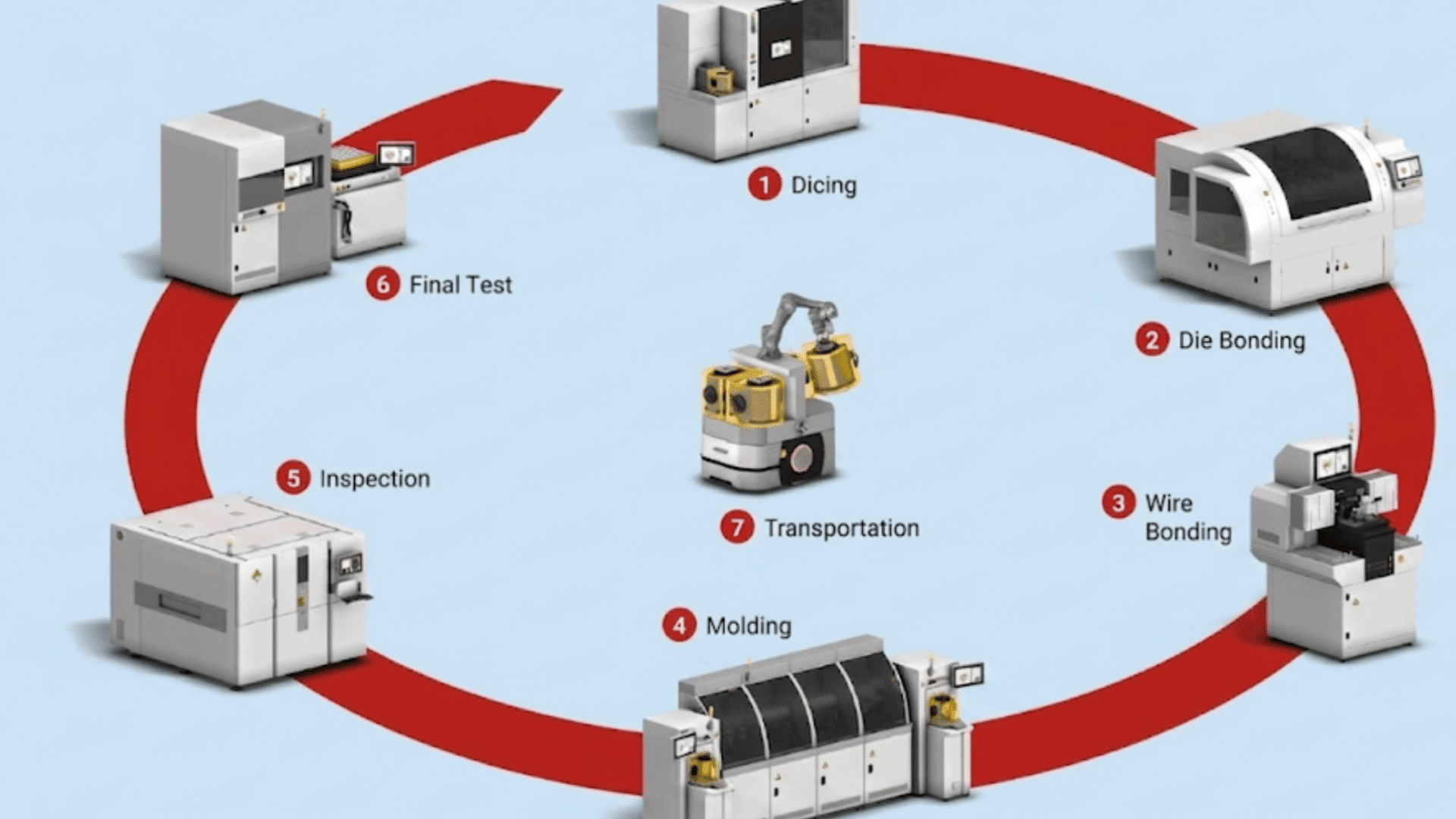
Semiconductor manufacturing uses advanced processes to turn raw silicon into powerful chips that support everyday electronics, computing systems, and modern technologies.
1. Silicon Wafer Manufacturing
The process begins with high-purity silicon extracted from raw materials and refined for semiconductor use.
The purified silicon is formed into large cylindrical crystals, sliced into thin wafers, and polished until the surface becomes extremely smooth.
These silicon wafers provide the foundation where complex electronic circuits are later created.
2. Oxidation and Thin Film Deposition
During this stage, manufacturers add thin layers of insulating and conductive materials onto the silicon wafer surface.
Processes like oxidation and deposition create protective layers and enable different electrical functions within the chip.
These layers form the foundation for building transistors, connections, and other microscopic circuit components.
3. Photolithography Process
Photolithography transfers detailed circuit patterns onto the wafer using light, masks, and photosensitive materials called photoresists.
The wafer is coated with photoresist, exposed to patterned light, and developed to reveal specific areas.
This step allows manufacturers to create the extremely small, precise designs needed for modern semiconductor chips.
4. Etching Process
Etching removes unwanted materials from the wafer surface to create the required circuit structures.
Manufacturers use chemical or plasma-based techniques to remove exposed layers while protecting selected areas.
This process shapes the tiny features that form transistors, electrical pathways, and other essential parts of a semiconductor device.
5. Doping and Ion Implantation
Doping modifies the electrical properties of silicon by adding controlled amounts of specific impurities.
During ion implantation, charged particles are inserted into selected areas of the wafer to improve conductivity and create transistor functions.
This step helps control how electricity flows through the semiconductor and enables the chip to operate.
6. Wafer Testing and Die Separation
After circuit creation, wafers undergo detailed inspections and electrical testing to identify defects and verify performance. Once approved, the wafer is cut into individual pieces called semiconductor dies.
Each die contains a complete circuit design and becomes the core component used in the final chip package.
7. Semiconductor Packaging and Final Testing
The individual semiconductor dies are placed inside protective packages that provide support, connections, and heat management.
Manufacturers attach electrical connections and perform final testing to ensure chips meet quality standards.
Tested chips are then prepared for integration into devices such as smartphones, computers, vehicles, and other electronic systems.
Why Is Semiconductor Packaging Important?
Semiconductor packaging plays a vital role in chip performance, improving speed, efficiency, and reliability while supporting advanced electronic technologies.
- Improves Chip Performance: Advanced packaging reduces signal delays, improves processing speed, and increases overall chip efficiency.
- Supports Smaller Devices: Modern packaging techniques allow manufacturers to create compact chips for smartphones, laptops, and other portable electronics.
- Enhances Energy Efficiency: Better packaging designs improve power management and help chips operate with lower energy consumption.
- Enables Advanced Technologies: Advanced packaging supports high-performance applications such as AI chips, data centers, and high-performance computing systems.
- Improves Reliability: Packaging protects semiconductor components from heat, damage, and environmental factors, helping devices perform consistently.
What Equipment Is Used in Semiconductor Manufacturing?
Semiconductor manufacturing uses advanced equipment to design, build, inspect, and test microscopic chip components with high precision.
| Equipment | Purpose | Role In Production |
|---|---|---|
| Lithography Machines | Transfer circuit patterns onto silicon wafers. | Create precise chip designs. |
| Deposition Systems | Add thin material layers to wafers. | Build chip structures and connections. |
| Etching Equipment | Remove unwanted wafer materials. | Form detailed circuit features. |
| Inspection And Testing Tools | Check chips for defects and performance. | Ensure quality and reliability. |
What Are Semiconductor Chips Used For?
Semiconductor chips are essential components that power modern electronics, vehicles, communication systems, and advanced technologies.
- Smartphones and Computers: Enable processing, memory storage, displays, and connectivity features in everyday electronic devices.
- Artificial Intelligence Systems: Power AI models, machine learning applications, and high-performance computing systems.
- Electric Vehicles: Control battery management, power systems, sensors, and advanced driving features.
- Medical Equipment: Support diagnostic machines, monitoring devices, and advanced healthcare technologies.
- Industrial Automation: Manage robotics, manufacturing systems, and smart factory operations.
- Communication Networks: Semiconductor chips power communication systems that use different cable types for reliable data transmission.
Major Semiconductor Manufacturing Hubs Around the World
Semiconductors are manufactured in global chip-making hubs such as Taiwan, South Korea, the United States, China, and Japan.
These countries operate specialized facilities called fabs (fabrication plants) that use advanced equipment, skilled engineers, and precise manufacturing processes to produce semiconductor chips.
Taiwan leads in advanced chip production, while South Korea specializes in memory chip manufacturing.
The U.S. leads in chip design and research, while China and Japan support production, materials, and equipment.
Governments are also investing in semiconductor production through initiatives such as the CHIPS Program to strengthen domestic chip manufacturing and supply chains
These regions collectively support the growing demand for electronic devices and emerging technologies.
What Are the Different Types of Semiconductor Packaging?
Semiconductor packaging types range from traditional designs to advanced solutions that improve chip performance, size, efficiency, and integration.
| Packaging Type | Category | Brief Description |
|---|---|---|
| Dual In-Line Package (DIP) | Traditional | Uses two rows of pins for simple chip mounting and reliable connections. |
| Quad Flat Package (QFP) | Traditional | A surface-mount package with leads on four sides for more connections. |
| Ball Grid Array (BGA) | Traditional | Uses solder balls underneath the package for better performance and a more compact design. |
| 2.5D and 3D IC Packaging | Advanced | Stacks or integrates multiple chips to improve speed and efficiency. |
| Chiplet Packaging | Advanced | Combines smaller chip units into one package for flexible chip designs. |
| Fan-Out Wafer-Level Packaging (FOWLP) | Advanced | Creates thinner, high-performance packages with increased integration. |
| System-in-Package (SiP) | Advanced | Combines multiple components, such as processors and memory, into one package. |
Why Is Semiconductor Manufacturing So Difficult?
Semiconductor manufacturing requires extreme accuracy, costly facilities, and advanced technology to produce reliable, high-performance chips.
- Extreme Precision Requirements: Chips contain microscopic circuits that require nanometre-level accuracy during manufacturing.
- Expensive Manufacturing Facilities: Semiconductor fabs need billions in investment, advanced equipment, and controlled cleanroom environments.
- Complex Supply Chains: Chip production relies on global suppliers for materials, equipment, and specialized technologies.
- Need for Advanced Technology: Manufacturers must continuously improve processes to create smaller, faster, and more efficient chips.
What Is the Future of Semiconductor Manufacturing?
The future of semiconductor manufacturing will focus on creating smaller, faster, and more efficient chips to support growing technology demands.
Smaller transistor designs will help improve performance while reducing power consumption.
Rising demand for AI applications will drive the production of specialized chips for machine learning and advanced computing.
Advanced packaging technologies, such as 3D ICs and chiplets, will improve chip integration and efficiency.
At the same time, countries and companies are expanding semiconductor supply chains to increase production capacity and reduce dependence on limited manufacturing regions.
Conclusion
Semiconductor manufacturing is a highly precise process that combines advanced engineering, specialized equipment, and global expertise.
Each stage, from chip design to testing, helps produce reliable electronic components.
With the growth of AI, electric vehicles, and smart technologies, semiconductor innovation will continue driving future advancements.
Learning about chip production reveals the complex technology that powers modern devices.
Being curious about semiconductor technology can help you find out how these essential components continue shaping the future of the digital world.
Frequently Asked Questions
How Much Does a Packaging Engineer Make at SpaceX?
A Packaging Engineer at SpaceX typically earns a competitive salary that varies by experience, location, skills, and level of responsibility.
Does the US Have Any Semiconductor Factories?
Yes, the US has semiconductor fabrication facilities (fabs) that produce advanced chips through companies like Intel, TSMC, Samsung, and Micron.
Do You Need a Degree to Be a Packaging Engineer?
Yes, most Packaging Engineer jobs require a bachelor’s degree in engineering, materials science, or a related field, along with relevant technical skills and experience.